![]()
![]()
New Microprocessor learning board demonstrates exemplary design of 8-bit single board computer. More peripheral and easy to adapt to be a dedicated controller.
I decided to rename C52EVB to be 8051SBC. Since the cpu can be any 8051 compatible chips with 40-pin DIP package. The old day chips, say 8031, 8751, 8032 or the new chips, 89C51, 89C52, 89C51RD2 can be used without any problem. Some may think that your old chips were useless, now you can use it for many projects. The monitor program of new 8051SBC was placed at external 32kB EPROM. With this space, you can customize your own monitor code or even add the application program and have the DIP switch to boot it when power up. The 32kB SRAM still be mapped as external code and data memory. We can test the program in RAM, when it firms then put it in the space in EPROM. The memory and i/o decoder is now using GAL (Generic Array Logic).
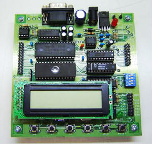
Figure 1: The prototype of 8051SBC (click for big picture).
The hardware schematic was provided to be an exemplary design for student to learn basic design of 8-bit microprocessor board. The board is a generic tool for every microprocessor lab. I provided all materials in public domain, so you may build it for your lab. Student can learn assembly programming, HLL programming and hardware interfacing.
The new 8051SBC features;
Hardware Schematic
- CPU: Any 8051 compatible with 40-pin DIP package @11.0592MHz
- MEMORY: 27C256, 32kB EPROM for monitor program
- 62256, 32KB SRAM for both code and data space
- I/O: direct cpu bus interface 2x16 line LCD
- 8-bit input port, 74LS244
- 8-bit output port, 74HC573
- MEMORY and I/O Decoder: GAL16V8D
- EEPROM: 24LC256, 32KB serial eeprom
- RTC: Real-time clock, DS1307 with +3V Lithium backup
- ADC: LTC1298, SPI interface 2-channel 12-bit Analog-to-Digital Converter
- I/O pins: P1,P3 of 8051 cpu, 16-bit I/O port
- Debug LED: single dot LED connected to P1.7
- Keypad and DIPSW: 4-bit keypad and 4-bit DIP switch
- RS232 Level Converter: MAX232
- RS485: 75176 differential transceiver
- Serial Interface: 9600 8n1
- Monitor Program: Modified PAULMON2 including new commands
Complete schematic for cpu and memory is shown in Figure 2. U7 is 40-pin 8051 compatible chip. The xtal is 11.0592MHz. JP1 selects internal or external code memory. With the external monitor mode, we make EA# to GND. The data bus D0-D7 are tied to memory chip, U1, U2 and to the GPIO, U3, U4 directly. Both memory chips are 32kB, so each chip needs A0-A14. A15 is used for memory decoder that decodes between first 32kB and second 32kB of external code memory. When A15 = 0, U1 the monitor rom was selected. The OE# of U1 is tied to PSEN#, so the code memory will enable only when address range 0x0000-0x7FFF of code memory are accessed. The upper memory space from address 0x8000-0xFFFF makes A15 = 1. When A15 = 1, U2 or SRAM will be selected. This memory space was decoded to be overlapped between external data and code memory. So while running under monitor mode, we can then load the hex code into the SRAM(data memory) and when JUMP from monitor program to address says 0x8000, the PSEN# that AND with RD# and ties to OE# of SRAM will enable the RAM to be code memory.
Since we have decoded the lower space, 0x0000-0x1FFF for code memory, this left a big space for external data memory from 0x0000-0x1FFF. The 8051SBC then borrowed this area to make the I/O that can access as the memory space with RD# and WR# combination with address decoder.
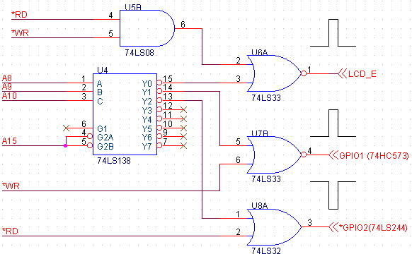
We can say that this area is memory mapped I/O. U3 is an 8-bit D-FF for output port. U4 is 8-bit tristate for input port. The LCD also connects cpu bus directly. To make the I/O decoder for each chip, we use A8, A9, A10 and A15 to select each block. The I/O map shows the address range for each device. U6 is PLD made from GAL16V8. It provides the memory and I/O decoder, later you will see details description on how to implement the decoder.
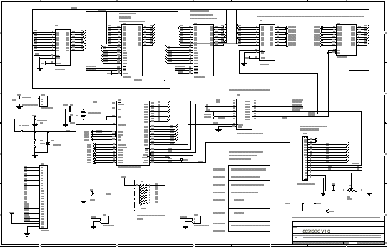
Figure 2: Complete hardware schematic, CPU, memory, PLD
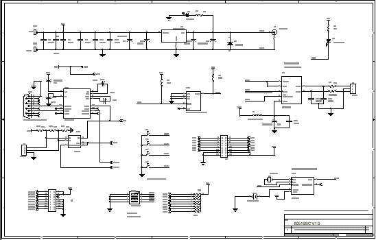
Figure 3: RS232, RS485, DC supply, EEPROM, ADC, RTC, keypad, debug LED.
U8 is +5V voltage regulator. D4 is protection diode. The RS232 level converter is MAX232. Notice that we have the RS485 transceiver as well. The TxD pin from CPU can tie to both input, T1IN (U10) and D(U12) directly. Howvere the RxD pin is the output of AND logic between R1OUT(U10) and R(U12). U11 is 32kB I2C EEPROM. It uses for program storage or the aplliaction program can use it. U9 is a popular 12-bit ADC having SPI interface. The reference voltage uses +5V. The two channels analog input has RC filter. U13 is RTC with I2C interface. It shares the I2C signal with EEPROM, U11. SW1 is 4-bit DIP swicth for system settings. User can use S3, S4, S5 and S6 for application program.
CPU list
I have tested some of 40-pin DIP package 8051 compatible CPU with the 8051SBC, table 1 shows the reason for each chip and you may find the right for your applications.
8751 old chip with ceramic package and quartz window for UV, new generation will see how the old chip look likes. 8031 romless 8051, 128 bytes RAM 8032 romless 8051, 256 bytes RAM 8052 basic interpreter with EA = +VDD AT89S8252 SPI, WDT, 2kB EEPROM, 8kB FLASH, 256 bytes RAM AT89C51 4kB FLASH 128 bytes RAM AT89C52 8kB FLASH 256 bytes RAM DALLAS DS500T 8kB loadable RAM RTC
Table 1: CPU that can be used with 8051SBC. GAL Decoder
The reason that took me to use GAL is to reduce the number of discrete gate for memory and i/o decoder. You may noticed that, with a C52EVB, only one chip, the 74HC00 was used for memory and 8255 decoder. However with new 8051SBC, I need to decode the LCD and simple port. This needs more chip, so better try with 20-pin popular GAL from Lattice, the GAL16V8D. The GAL can emulate logic function and can reprogram many times.
Before getting into GAL's matter, let begin with how to replace the logic gate using logic equation. Now let see the actual decoder circuit. First take a look for memory decoder.
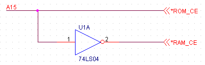
The EPROM will place at 0x0000 to 0x7FFF. And the SRAM will place at 0x8000 to 0xFFFF. We see that we can use A15 to be a chip select control signal for EPROM directly. Whereas for the SRAM it needs to invert A15 in order to select SRAM when A15 becomes '1' for address 0x8000-0xFFFF.
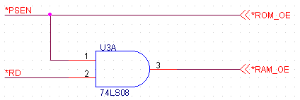
Note * is active low signal. To read or fetch the content of EPROM, the place we store monitor program, we must provide *PSEN signal tied to output enable pin.
However for SRAM, we will use it for user program running as well as the place where we can edit the machine code, so we must make it to be code and data memory space. This can be made easily with *RD and *PSEN logical AND together. The circuit would be,
A bit complicate for i/o decoder, as shown below we see the popular decoder chip, the 74LS138, 3-to-8 line decoder and some gates were used to provide control signal for the i/o devices. The i/o space uses the external data memory with address 0x0000 to 0x7FFF. A15 must be low to enable the output of 74LS138. A8-A10 selects the active low output for each i/o. Let look at the first device, the LCD. Y0 will active low when all inputs are low, or A8-A10 and A15 = '0'. The datasheet of LCD says, the signal E of LCD will active for both read or write cycle, so we AND them together with U5B. U6B provides the positive pulse when Y0 and pin 6 of U5B low. This signal, LCD_E can then directly tie to signal E of the LCD.
Similarly for GPIO1 or 74HC573, latch signal. Now GPIO1 uses Y1, that means A8 must be '1', A9,A10 and A15 must be '0'. The WR signal is logical OR with Y1. The NOR gate U7B provides the positive pulse similar to the LCD_E signal. This signal will control the D FF latch. Dada is loaded into FF and the is latched at high to low transition.
For the input port made by tri-state buffer, 74LS244, the enable signal was made by Y2 and RD signal. However now A9 must be '1' and A8, A10 and A15 must be '0'.
With above decoder, we then need more chips to make it. Now let see how the GAL chip looks like.
GAL16V8D
The GAL chip was Lattice GAL16V8D. The GAL is a programmable logic device (PLD). We can write the logic equation, convert it to JED file and program the GAL with JED file. Then we can replace above circuit with single GAL chip. The GAL16V8 has 10 inputs and 8 outputs. The chip can reprogram many times. In this design I used only one chip to replace such memory and i/o decoder circuit.
Using PLD Assembler
To implement the logic with GAL, we must first edit the logic equation and have the PLD assembler to translate the equation file to JEDEC file. I found OPALjr 2.0 from google search. It's very easy to use. Now let see the equation of above decoder.
; 8051SBC PLD Equation
; Memory and I/O decoder for 8051 Single Board Computer
; Wichit Sirichote, kswichit@kmitl.ac.th
; May 1, 2003
; PLD: Lattice GAL16V8DCHIP 8051SBC GAL16V8
a15=1 rd=2 wr=3 a8=4 a9=5 a10=6 rs232=7 rs485=8 psen=9 rom_ce=12
ram_ce=13 ram_oe=14 rom_oe=15 lcd_e=16 gpio1=17 gpio2=18 rxd=19EQUATIONS
ram_oe = rd * psen
rxd = rs232 * rs485
rom_ce = a15
ram_ce = /a15
rom_oe = psen
/lcd_e = rd * wr + a8 + a9 + a10 + a15
/gpio1 = /a8 + a9 + a10 + a15 + wr
gpio2 = a8 + /a9 + a10 + a15 + rd
Note. * is logical AND, + is logical OR and / is logical NOT.
There is some i/o pin available on GAL, I also used them for sharing between rs232 and rs485. The output is tie to RxD pin of the cpu. See schematic for detail.
When finish editing the equation file, click MODULE -> EQU2JED, it will convert the equation file to JEDEC file. Let look at the output JEDEC file.
GAL16V8
EQN2JED - Boolean Equations to JEDEC file assembler (Version V101)
Copyright (c) National Semiconductor Corporation 1990-1993
Assembled from "D:\C52EVBV3\O\8051SBC.EQN". Date: 5-1-103
*
NOTE PINS a15:1 rd:2 wr:3 a8:4 a9:5 a10:6 rs232:7 rs485:8 psen:9*
NOTE PINS rom_ce:12 ram_ce:13 ram_oe:14 rom_oe:15 lcd_e:16 gpio1:17*
NOTE PINS gpio2:18 rxd:19*
NOTE GALMODE SMALL*
QF2194*QP20*F0*
L0000
11111111111111111111011101111111*
L0256
11111111011111111111111111111111
11111111111110111111111111111111
11111111111111110111111111111111
11011111111111111111111111111111
01111111111111111111111111111111*
L0512
11111111101111111111111111111111
11111111111101111111111111111111
11111111111111110111111111111111
11011111111111111111111111111111
11110111111111111111111111111111*
L0768
01110111111111111111111111111111
11111111011111111111111111111111
11111111111101111111111111111111
11111111111111110111111111111111
11011111111111111111111111111111*
L1024
11111111111111111111111111110111*
L1280
01111111111111111111111111110111*
L1536
11101111111111111111111111111111*
L1792
11011111111111111111111111111111*
L2048
11001111*
L2128
1000000011111000111110001111100010000000100000001000000010000000*
L2192
10*
C5053*
0000The JEDEC file is standard file for any GAL programmer. I used GALBLAST to program it.
Before you can use GAL or any PLD efficiently, you must have knowledge on the fundamental of digital logic. The PLD is just to help hardware design more easy.
12-bit ADC converter
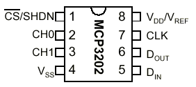
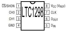
I found Microchip 12-bit ADC converter, MCP3202 that can replace Linear Technology LTC1298 directly. Below is pin diagram of 8-pin DIP package. MCP3202 is cheaper than LTC1298. Both chips are pins compatible. The 8051SBC can use either one without any problem.
Software
With the external 32kB EPROM, the 27C256, we then need the EPROM programmer. I used willem EPROM programmer. Also here in Thailand http://se-ed.net/mpu51/ You may build it easily. Later I'll add the EPROM programmer attach to the 8051SBC.
The main monitor code space is approx. 8kB. This fits exactly in 89C52 chip. So you can add many things into 32kB EPROM. During firmware developing, I used parallel eeprom, 28C256 from ATMEL. I made the adapter from two sockets. The socket swaps pin 1 and pin 14. If you have the 28C256, you can use my idea.
Some may got many ceramic EPROM, 27C256. To erase it, you need Ultraviolet light. When your code firms, you can write the program into a cheap 27C256 OTP (One Time Program).
The monitor program composes of three files.
1. 8051SBC.ASM
2. myextra1.ASM
3. new.cThe 8051SBC.ASM and myextra1.asm are modified version of PAULMON2 free monitor program written by Paul Stoffregen. Both files fit in 8kB space. The new commands is now under developing with Micro-C compiler. The available for download was tested on RAM and then recompile with MEDIUM memory model. In addition to such monitor code, I also experimented with Camel FORTH. EEPROM booting still working with this version excepts the boot switch is now move to DIP switch bit 0. To start Cemel FORTH, when set DIP switch bit 1 to '0' after power up, it will enter Camel FORTH.
The Intel hex file for the monitor program including new commands and Camel FORTH is here, 8051SBC.HEX.
Below is the sample of new commands.
8051SBC Microprocessor Learning Board ADDR:8000> Help
Standard Commands
?- This help list
M- List programs
R- Run program
L- Download
U- Upload
N- New location
J- Jump to memory location
H- Hex dump external memory
I- Hex dump internal memory
E- Editing external ram
C- Clear memory
User Installed Commands
D- Disassemble
S- Single-Step
Q- Quick home
Z- ZAP EEPROM
W- NEW COMMANDSADDR:8000>
Notice that letter D is now changed to Disassemble, and L changed Load Intel hex file. Command Q will get back to address 0x8000. Z command still exists. Now let see new command with letter W.
ADDR:8000> NEW COMMANDS
8051SBC new commands (press ? for help or q to quit)
>>
Help Menu
A ASCII Table
D Dec2Hex
R Read GPIO2
Q Quit
I i/o address
B Binary image
? help>>Decimal to Hex converter
Enter decimal number = -32768
Dec -> Hex -> Bin
-32768 -> 8000 -> 1000000000000000>>Read GPIO2 (8-bit input port)
FD 11111101
>>i/o address decoded by PLD
LCD command write 0x0000
LCD data write 0x0001
LCD command read 0x0002
LCD data read 0x0003
GPIO1 8-bit output port 0x0100
GPIO2 8-bit input port 0x0200
expansion i/o space 0x0300-0x07FF>>
Now let make DIP switch bit 1 to '0' and then power up the board.
8051 CamelForth v1.6 27 Mar 2000
ok
2a emit *ok
ok
: star 2a emit ; ok
ok
ok
star *ok
ok
okThe sample above is a common first word for FORTH beginner. We define word 'star' with 2a put to data stack and emit it to screen. I used to try FORTH with my design 80C88, since I was a student in 1984. However the Harvard architecture of 8051 may not suitable to make use of FORTH more efficient. The reason why I added FORTH to the 8051 board is just to experiment the startup booting.
Download
Schematic 8051SBC.pdf Monitor program 8051SBC.asm
myextra1.asm
new.cIntel Hex files mypaulm2.hex
myextra1.hex
new.hexIntel Hex file (three files) 8051SBC.hex 8051SBC Reference Manual 8051SBCreference.pdf PCB gerber files 8051gerber.zip OrCAD 9.1 MAX file 8051sbc.max OrCAD 9.1 Schematic and Netlist files orcad8051sbc.zip 8051SBC BOM bom8051sbc.txt Equation and JEDEC file for GAL16V8D 8051sbc.eqn
8051sbc.jedContribution to 8051SBC
- SBC51Lib.zip A library file for LCD module on SBC51 written by Muhammad Kamran,
Department of Electronics, University of Peshawar, NWFP, Pakistan.
 30 Nov 2003